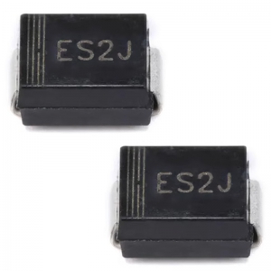
SMA packaging is a common type of surface mount (SMD) diode and transistor packaging. This type of packaging has been widely used in the electronics industry due to its durability, moderate size, and good heat dissipation performance. SMA packaging is particularly suitable for high-frequency and high-power applications.
characteristic:
Medium to high power processing capability: SMA packaging is designed to handle medium to high power levels and is suitable for power management, radio frequency (RF) applications, and other applications that require high currents.
Good thermal performance: There is a large metal pad at the bottom of the package that can be directly connected to the heat dissipation copper foil on the PCB, helping to effectively transfer heat from the internal semiconductor chip to the external environment.
Surface mount: SMA packaging is specifically designed for surface mount technology, which means it can be automatically assembled onto printed circuit boards, improving production efficiency.
Durable and sturdy: The SMA packaging structure is sturdy and suitable for use in harsh environments such as high temperatures or high vibration conditions.
Structure:
SMA packaging usually consists of a ceramic shell and an internal metal substrate, which contacts the semiconductor chip and plays a role in heat dissipation. The top of the package may have additional metal sheets or other heat dissipation enhancement structures. Pins extend from one side of the package for electrical connections.
Size:
The size of SMA packaging may vary depending on the specific manufacturer and product model, but usually follows industry standards. Generally speaking, the size of SMA packaging is roughly within the following range:
Package length: usually between 2.6mm and 3.2mm.
Package width: usually between 2.0mm and 2.6mm.
Package thickness: usually between 1.0mm and 1.5mm.
Application:
SMA packaging is commonly used in diodes (including rectifier diodes, Schottky diodes, voltage regulators, etc.), transistors, radio frequency (RF) devices, and other power semiconductor devices. These devices are widely used in power supply, radio frequency communication, consumer electronics, automotive electronics, industrial control, and other medium to high power electronic devices.
matters needing attention:
When designing and soldering SMA packaging, the following points need to be noted:
Pad design: PCB design needs to be based on the pad layout provided by the manufacturer to ensure correct soldering and alignment.
Welding process: The welding of SMA packaging requires precise temperature control and time management to avoid overheating or cold welding.
Thermal management: In medium to high power applications, heat dissipation issues must be considered and may require the use of cooling solutions such as heat planes, heat sinks, or fans.
When selecting SMA packaging, reference should be made to the manufacturer's data manual and application notes for detailed dimensional information, recommended design guidelines, and welding process parameters. SMA packaging is very popular in the design of medium to high power electronic products due to its high power processing capacity and good heat dissipation performance.
Shenzhen Baoxin Chuang Electronics Co., Ltd.
Address: 45th Floor, SEG Plaza, 1002 Huaqiang North Road, Futian District, Shenzhen, Guangdong, China
Website: www.boxintron-ic.com
Tel: +86-0755-8355 3623/8322 8690/8322 8629/8322 8357
Fax: +86-0755-8366 0820
Email: service@boxintron.com
Electronic components with a single expert
Shenzhen Baoxin Chuang Electronics Co., Ltd. is committed to becoming the best IC supplier with single expert and IC agent
Strive to provide customers with one-stop electronic components procurement and IC supporting services
Tel: +86-0755-8355 3623 Fax Fox: +86-0755-8366 0820 Email: service@boxintron.com
Address: Room 4503, 45th Floor, SEG Plaza, 1002 Huaqiang North Road, Futian District, Shenzhen, Guangdong, China
![Shenzhen Baoxin Chuang Electronics Co., Ltd. [one-stop type of electronic components with one-only original authentic] Shenzhen Baoxin Chuang Electronics Co., Ltd. [one-stop type of electronic components with one-only original authentic]](templates/web/images/logo.png)